In the influence of an increase in ambient temperature few electrons in the valence band acquire sufficient energy and escape to the conduction band. The gap between this valence band and highest energy band (conduction band) is termed as band gap. We will find ways to control this.
Introduction
In this series we have been talking a lot about rectifier diodes , tunnel diodes and also the concept of half and full wave rectification . Now we will learn something about zener diodes.
A frequent problem encountered with zener diodes is the effect of ambient temperature and supply voltage variations. This problem usually gets serious if the circuit involves critical comparison between zener reference voltage and an unknown value.
In this article we will find out how a zener diode can be “reinforced” with additional electronic parts to countermand the changes in ambient temperature and other factors. But it will be first interesting to know regarding band gap.
What is Band Gap
The basic configuration of a semiconductor atom (zener diode in this case) shows two distinct energy bands of four outer electrons. Conduction of electrons begins in the highest energy band with increase in temperature. The electrons are agitated due to increasing heat to an extent that they free themselves from the valence band and “jump” into the conduction band. This gap between the valence and the conduction band is termed as band gap. The phenomenon leads to a change in the value of the zener diode and ultimately a circuit malfunction.
Following are two ways to cancel out the above effect in a zener diode.
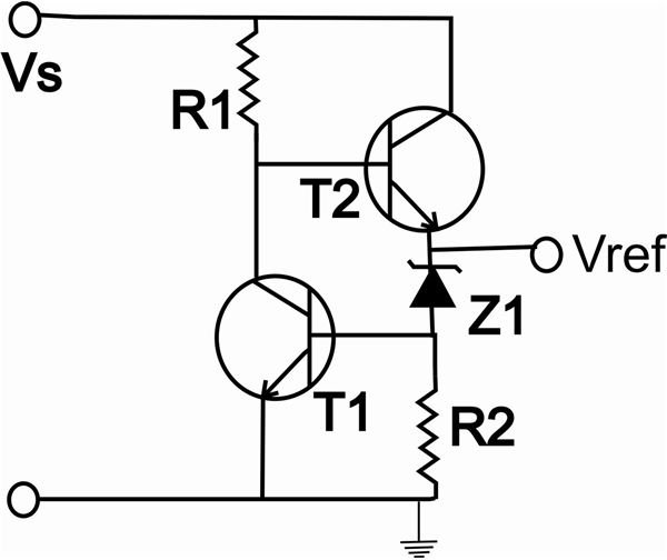
Using a Zener-Transistor Combination
Referring to the figure at left, if there’s an significant increase in the ambient temperature, the zener diode starts conducting more and thus lowering its value. Due to this forced conduction, the potential difference across R2 rises. When it reaches above 0.6 volts T1 conducts to reduce the base current of T2, so that its emitter is unable to provide enough current to the zener.This inhibits the excess flow of current through the zener and its value is corrected. This circuit is almost a perfect regulator of zener diode reference voltage.
Using Current Mirror Transistors
Another very precise voltage reference can be created using two current mirror transistors. A constant current source is generated by these transistors. The resistor at one of the transistors emitter is dimensioned to produce the required reference voltage. Another resistor which is connected in series with the supply voltage is also selected such that a potential difference of precise1.2 volts is formed across it, this is called the band gap reference voltage.
Any variation in the ambient temperature causes the potential across the emitter resistor of the current mirror transistor to change. This difference of voltage is sensed by the third transistor which compensates by pulling down any rise in current through the current mirror transistor and thus nullifying the external effects of temperature or voltage variations.
How to Test a Zener Diode?
Wondering how to test a zener diode? Well, a zener diode can be very easily tested through the following explained simple procedure:
-
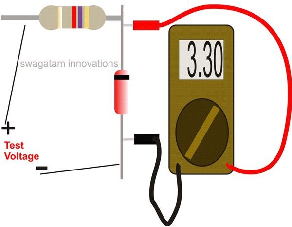
Take a resistor of any value between 1K and 10 K.
-
Connect it to the cathode (the lead on the banded side) of the zener diode, either by twisting or soldering.
-
Now, apply a voltage across the resistor’s free end and the zener anode terminal.
-
The applied voltage should be greater than the zener rated voltage by at least 1 volt, i.e. if the zener voltage is 3, then the minimum applied voltage should be at least 4 volts or more.
-
Now, using a digital multi meter, measure the voltage across the zener terminals.
-
The reading should be almost (+/- 2%) equal to the rated zener voltage.
-
Any other value indicates a faulty diode.