The roots of semiconductor behaviour lie in their unique crystal lattice and the way the atoms are arranged inside the lattice structure. Learn about these aspects in this article.
Introduction
We have been studying the basics of digital electronics in the form of Bohr’s atomic structure theory, energy bands , conduction band, Pauli’s principle in relation to quantum numbers and so forth. Now the stage is set that we proceed towards more advanced concepts about semiconductors which form the core of basic digital electronics. We will start by talking about the definition of semiconductors and what they are all about.
Classification of Materials
Different materials have difference electrical characteristics and this leads to their classification in any of the three categories which are as follows.
Insulators are materials which do not conduct electricity. But how do we explain this in terms of the theory we have already learned in the lessons mentioned above. Well stated along those lines, an insulator simply means a material which does not have any free electrons available for carriage of current. This is because the valence band electrons of these materials are bound very tightly to their parent nuclei and require vast amounts of energy to break that bond. In other words these materials have a large forbidden energy gap. Of course this effect could be overcome to some degree when energy is supplied to these tightly bound electrons in the form of say heat. This means that at higher temperatures there might be a slight conduction available in them.
Conductors are materials which lie on the other end of the spectrum and the forbidden energy gap is literally zero. This in effect means that the valence and conduction bands of these atoms are literally overlapping with each other so there is hardly any restriction of electrons to jump to and from these bands.
Semiconductors are midway between insulators and conductors. In these materials the energy gap is neither very large like insulators nor negligible like conductors. There is a moderate energy gap which does not require much energy for the electrons to jump from valence to conduction band. The conduction band of these materials is nearly empty if not fully empty. At a temperature of zero degrees Kelvin these materials act as insulators since there are no electrons in the conduction band but at room temperature the forbidden energy gap is reduced to a minimal. Infact the typical values of the energy gap in a semiconductor is of the order of 1 eV.
Another thing that separates these materials from conductors is that while the current in a conductor is solely due to the flow of electrons; the current in a semiconductor is not only due to flow of electrons but also due to flow of holes about which we learnt previously. The electrons flow across the conduction band whilst the holes flow via the valence band only.
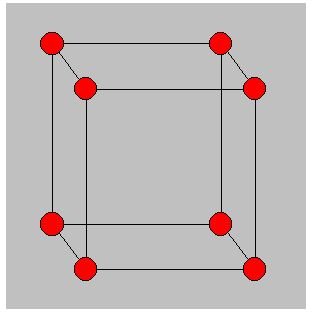
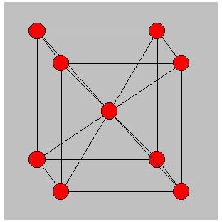
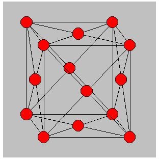
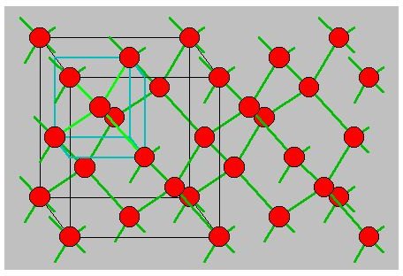
The typical properties of the above mentioned category of materials are due to their unique structure which is known as the lattice structure and basically it consists of a repeated arrangement of atoms in a particular geometric pattern. There are several different types of crystal structure such as the Simple Cubic structure, Base Centered Cubic structure, Face Centered Cubic structure and Diamond structure.
-
In SC structure the lattice is in the form of a cube having an atom at each of its vertices. The only material which exists in SC form is Podium.
-
In BCC the atoms are at the vertices of the cube plus one atom at the center of cube, hence each atom has 8 neighbours. E.g. Sodium
- In FCC there are atoms at the corners of the cube as well as the centers of each of the faces thus giving a figure of 12 atoms in the neighbourhood of each atom.
-
Diamond lattice - the structure of semiconductors is slightly different and the semiconductor materials such as Silicon and Germanium have a structure known as the diamond lattice wherein there are four equidistant neighbours of each atom in the form of a tetrahedron.
We will learn more about the types of semiconductor materials and the role of the crystal structure in determining properties such as atomic binding in separate articles.
Image Credits
Department of Electrical, Computer, and Energy Engineering at the University of Colorado Website