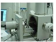
A Scanning Electron Microscope is a scientific instrument that is used to observe fine details of materials. SEM was introduced as a solution to low resolutions of optical microscopes and used to examine very small surfaces up to the nanometer level.
The Scanning Electron Microscope (SEM) is a scientific instrument that is used to examine objects on a very fine scale. Unlike many other microscopes, SEMs use a beam of highly energetic electrons to examine objects. It has a very high resolution compared to the best Light Microscopes. Generally SEMs are capable of revealing the details of surfaces with 1 to 5 nanometer in size (1 nanometer = 10-9 m). Therefore Scanning Electron Microscopes are widely used for scientific observations of surfaces to gain details about shape, size, texture, composition, atomic arrangement, etc. in various materials.
History of Scanning Electron Microscope
Electron microscopes were developed as a result of the limitations of Light Microscopes. Light Microscopes have a theoretical limit of resolution that is about 500x or 1000x magnification and a resolution of 0.2 micrometers. This theoretical limit was reached in the early 1930s, and there was a need for better microscopes for examining fine details of materials. The first electron type of microscope was developed in 1931 in Germany by Max Knoll and Ernst Ruska. It was a Transmission Electron Microscope (TEM) that is similar to Light Microscopes except for the fact that it used electron beams to see through the object. The first commercial SEM was introduced in 1965 by the Cambridge Instrument Company and was developed by Professor Sir Charles Oatley and his student Gary Stewart.
Principals of Scanning Electron Microscope
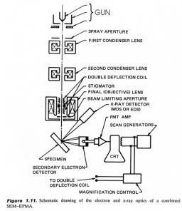
In a SEM, accelerated electron beams with a high kinetic energy (from several hundreds to 40,000 Volts) are emitted from an electron gun and used to scan the surface of the specimen (the object to be scanned). One or two condenser lenses are used to focus the electron beam to a spot about 0.4 nm to 5 nm in diameter. Once these electrons have reached the surface of the specimen, the energy of the electrons is dissipated in a variety of forms producing secondary electrons (these produce SEM images), back scattered electrons (these are incidental electrons that are reflected backward), X-rays, Auger electrons, elastically scattered electrons, and inelastically scattered electrons. Each of these can be examined by various methods, and each of them has special scientific use. For example, diffracted backscattered electrons are used to determine crystaline structures and the orientation of minerals. The signals emitted from the surface of the object are detected and amplified using a special amplifier. Then it is sent to a CRT display. In modern SEMs the signals are digitally recorded and displayed on a computer monitor and saved to a computer’s hard disk.
Applications of Scanning Electron Microscope
SEMs are used for scientific observations of materials for various practices. Topography, morphology, composition, and crystallographic details are some information frequently detected using Scanning Electron Microscopes. Topography or texture (how an object looks) has a direct relation to its material properties like hardness and reflectivity, etc. The shape and size of particles or morphology is related to properties like strength, ductility, etc. These are very important aspects of materials that are subjected to number of ongoing researches and other purposes. Also crystallographic information (how atoms are arranged in a material) and details about compositions are quite useful for scientific purposes. Therefore SEMs has been popular among researchers, academics, and related industries.
SEMs are also widely used for chemical analysis like spatial variations in chemical compositions and qualitative chemical analysis. Three dimensional data also can be measured using SEMs. Photogrametry and Photometric stereo are two methods that can be used to measure 3D data. They have applications like corrosion measurement, roughness measurement, and measurement of fractal dimension.
There are several limitations of Scanning Electron Microscopes. Samples must be in solid form and the dimensions are limited, since it must be able to fit the microscope. There are number of materials, like organic materials, that can’t be observed using Scanning Electron Microscopes . Despite these drawbacks it is the most important and the most popular type of microscope today.
This post is part of the series: Testing of Materials
Testing of materials is an extremely important in Materials science. Also it quite important in many scientific activities. In this article series material testing instruments, testing methodologies and their importance are discussed.