What is a timing diagram? What is the importance of timing diagram with respect to a microprocessor? The answer for above questions can be found here. Learn in detail about the timing diagram and the various states in 8085 microprocessors.
Introduction
Timing plays a crucial role, not only in sports like cricket but also in digital electronic equipments like microprocessors. Timing and Timing diagram plays a vital role in microprocessors.
What is a timing diagram? What role it plays with respect to microprocessors? Let’s discuss about these concepts in detail.
What is a Timing Diagram?
The timing diagram is the diagram which provides information about the various conditions of signals such as high/low, when a machine cycle is being executed. Without the knowledge of timing diagram it is not possible to match the peripheral devices to the microprocessors. These peripheral devices includes memories, ports etc. Such devices can only be matched with microprocessors with the help of timing diagram.
Before dealing with timing diagram, we have to make ourselves familiar with certain terms.
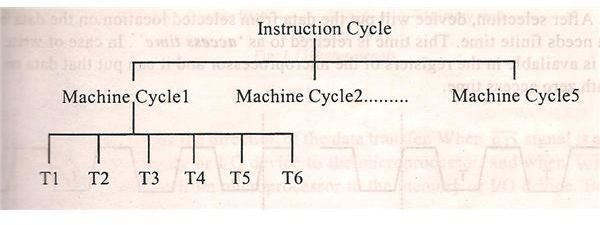
Instruction cycle:
Assume that the microprocessor is executing an instruction. Instruction cycle is nothing but the time taken to complete the execution of that instruction by the microprocessor. The 8085 instruction cycle consists of 1 to 6 machine cycles.
Machine Cycle:
Machine cycle is nothing but the time required to complete one operation of accessing memory, I/O. It is also the time required to complete one operation of acknowledging an external request. One machine cycle may consist of 3 to 6 T-states.
T-state:
T-state is nothing but one subdivision of the operation performed in one clock period. These subdivisions are internal state of the microprocessor synchronized with system clock.
Now let us discuss the timing diagram for various signals that are associated with 8085 microprocessor.
Timing diagram of various signals
Address latch enable:
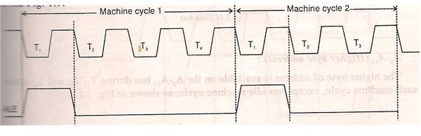
Address latch enable is an active high signal. (i.e.) the latch becomes enabled when the signal is high. It is activated during the beginning of T1 state of each machine cycle and it remains active in the T1state. But in case of bus idle machine cycle it is not activated.
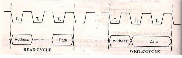
Data Bus (D0-D7):
While dealing with data bus, two types of data flow are possible. The data can be transferred from memory to microprocessor and vice versa.
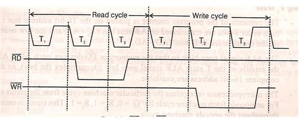
This process occurs during the T2 and T3 states.
There are 2 cycles. One is Read machine cycle and the other is write machine cycle. In read machine cycle, the data will appear during the later part of T2 state, while in Write machine cycle the data will appear on the beginning of T2 state.
But for reading a data from memory or I/O device, first we need to select the required device. After selecting the device, the required data to be read or written is taken from the selected location and placed on data bus. A certain amount of time is required to perform this action. This time is called “access time”. But for write cycle the access time is 0. This is because the data to be written is present on the registers of microprocessor and so it can put the data directly to data bus without any time delay.
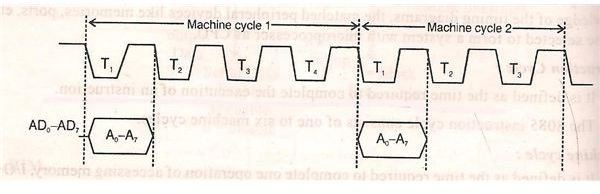
Lower byte address (A0-A7):
The lower byte of address is available on the time multiplexed address/date bus during the T1 state of machine cycle, except the bus idle machine cycle.
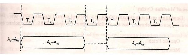
Higher byte addresses (A8-A15):
The higher byte addresses (A8-A15) is available for T1, T2 and T3 states of each machine cycle, except the bus idle machine cycle.
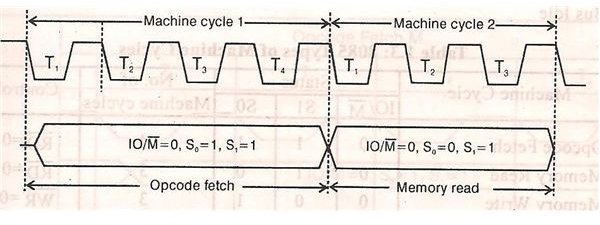
IO/M’, S0, S1:
From the previous discussions about 8085 microprocessor, we very well know that IO/M’, S0, S1 are the status signals of the microprocessor. These status signals decide the type of machine cycle is to be executed. So they remain activated from the beginning T1 state of a particular machine cycle and remains till the end of that machine cycle.
RD’ and WR’:
These 2 signals RD’ and WR’ decides the direction of the data transfer.
RD’ is Active: When RD’ goes active, the data is transmitted from memory, I/O device or any other peripherals to the microprocessor.
WR’ is active: When WR’ goes active, the data is transmitted from microprocessor to the memory or any other peripheral devices.
Now there might be a question arising within your mind.
Can both the signals become active at same time? The answer for this question is NO. In 8085 microprocessor either RD’ goes high or WR’ goes high. Both cannot take place at same time.
The data transfer both RD’ and WR’ takes place during T2 and T3 states of machine cycle. So these signals are activated during the T2 and T3 states.
In the next article let us explore the various types of machine cycles that are used in timing diagram.
Image Courtesy:
“Microprocessor and Its applications” by Manoharan