Internal Architecture of 8085 Microprocessor - Learn about the TCU, Flag and other components
Introduction
In the previous articles we learnt about what are microprocessors in general and the about the 8085 microprocessor in particular. We saw the various registers used in 8085 microprocessor and how they act along with Arithmetic and Logic unit to process a data. But Registers and ALU alone cannot successfully process a data and provide the result to the programmer. There are various other units which help in data transfer and addressing, Carry operation while adding or subtracting, and sometimes also to interrupt a process when necessary. Let us discuss about those units in detail.
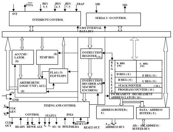
Architecture Diagram
Flags
Flags are nothing but a group of individual Flip-flops. The flags are mainly associated with arithmetic and logic operations. The flags will show either a logical (0 or 1) (i.e.) a set or reset depending on the data conditions in accumulator or various other registers. A flag is actually a latch which can hold some bits of information. It alerts the processor that some event has taken place.

But why are they called flags?
The possible solution is from the small flags which are found on the mail boxes in America. The small flag indicates that there is a mail in the mail box. Similarly this denotes that an event has occurred in the processor.
Intel processors have a set of 5 flags.
- Carry flag
- Parity flag
- Auxiliary carry flag
- Zero flag
- Sign flag
Consider two binary numbers.
For example:
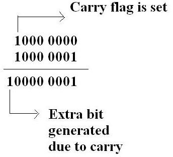
1100 0000
1000 0000
When we add the above two numbers, a carry is generated in the most significant bit. The number in the extreme right is least significant bit, while the number in extreme left is most significant bit. So a ninth bit is generated due to the carry. So how to accommodate 9th bit in an 8 bit register?
For this purpose the Carry flag is used. The carry flag is set whenever a carry is generated and reset whenever there is no carry.

But there is an auxiliary carry flag? What is the difference between the carry flag and auxiliary carry flag?
Let’s discuss with an example. Consider the two numbers given below
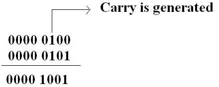
0000 0100, 0000 0101
When we add both the numbers a carry is generated in the third bit from the least significant bit. This sets the auxiliary carry flag. When there is no carry, the auxiliary carry flag is reset.
So whenever there is a carry in the most significant bit Carry flag is set. While an auxiliary carry flag is set only when a carry is generated in bits other than the most significant bit.

Parity checks whether it’s even or add parity. This flag returns a 0 if it is odd parity and returns a 1 if it is an even parity. Sometimes they are also called as parity bit which is used to check errors while data transmission is carried out.
Zero flag shows whether the output of the operation is 0 or not. If the value of Zero flag is 0 then the result of operation is not zero. If it is zero the flag returns value 1.
Sign flag shows whether the output of operation has positive sign or negative sign. A value 0 is returned for positive sign and 1 is returned for negative sign.
Instruction Register and Decoder
Instruction register is 8-bit register just like every other register of microprocessor. Consider an instruction. The instruction may be anything like adding two data’s, moving a data, copying a data etc. When such an instruction is fetched from memory, it is directed to Instruction register. So the instruction registers are specifically to store the instructions that are fetched from memory.
There is an Instruction decoder which decodes the informations present in the Instruction register for further processing.
Timing and Control Unit
Timing and control unit is a very important unit as it synchronizes the registers and flow of data through various registers and other units. This unit consists of an oscillator and controller sequencer which sends control signals needed for internal and external control of data and other units.
The oscillator generates two-phase clock signals which aids in synchronizing all the registers of 8085 microprocessor.
Signals that are associated with Timing and control unit are:
Control Signals: READY, RD’, WR’, ALE
Status Signals: S0, S1, IO/M’
DMA Signals: HOLD, HLDA
RESET Signals: RESET IN, RESET OUT
Interrupt Control
As the name suggests this control interrupts a process. Consider that a microprocessor is executing the main program. Now whenever the interrupt signal is enabled or requested the microprocessor shifts the control from main program to process the incoming request and after the completion of request, the control goes back to the main program. For example an Input/output device may send an interrupt signal to notify that the data is ready for input. The microprocessor temporarily stops the execution of main program and transfers control to I/O device. After collecting the input data the control is transferred back to main program.
Interrupt signals present in 8085 are:
INTR
RST 7.5
RST 6.5
RST 5.5
TRAP
Of the above four interrupts TRAP is a NON-MASKABLE interrupt control and other three are maskable interrupts.
A non-maskable interrupt is an interrupt which is given the highest priority in the order of interrupts. Suppose you want an instruction to be processed immediately, then you can give the instruction as a non-maskable interrupt. Further the non-maskable interrupt cannot be disabled by programmer at any point of time.
Whereas the maskable interrupts can be disabled and enabled using EI and DI instructions. Among the maskable interrupts RST 7.5 is given the highest priority above RST 6.5 and least priority is given to INTR.
Serial I/O control
The input and output of serial data can be carried out using 2 instructions in 8085.
SID-Serial Input Data
SOD-Serial Output Data
Two more instructions are used to perform serial-parallel conversion needed for serial I/O devices.
SIM
RIM
Address buffer and Address-Data buffer
The contents of the stack pointer and program counter are loaded into the address buffer and address-data buffer. These buffers are then used to drive the external address bus and address-data bus. As the memory and I/O chips are connected to these buses, the CPU can exchange desired data to the memory and I/O chips.
The address-data buffer is not only connected to the external data bus but also to the internal data bus which consists of 8-bits. The address data buffer can both send and receive data from internal data bus.
Address bus and Data bus:
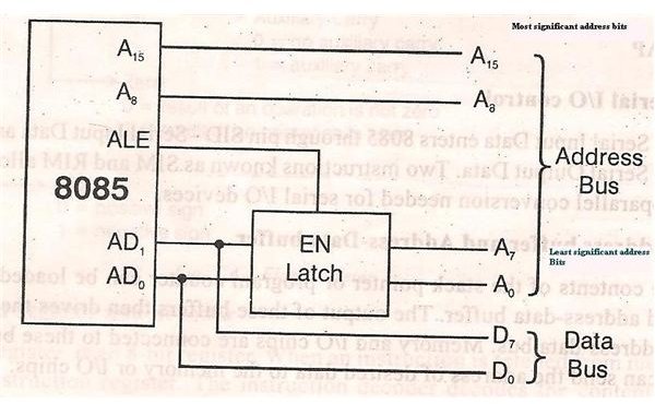
We know that 8085 is an 8-bit microprocessor. So the data bus present in the microprocessor is also 8-bits wide. So 8-bits of data can be transmitted from or to the microprocessor. But 8085 processor requires 16 bit address bus as the memory addresses are 16-bit wide.
The 8 most significant bits of the address are transmitted with the help of address bus and the 8 least significant bits are transmitted with the help of multiplexed address/data bus. The eight bit data bus is multiplexed with the eight least significant bits of address bus. The address/data bus is time multiplexed. This means for few microseconds, the 8 least significant bits of address are generated, while for next few seconds the same pin generates the data. This is called Time multiplexing.
But there are situations where there is a need to transmit both data and address simultaneously. For this purpose a signal called ALE (address latch enable) is used. ALE signal holds the obtained address in its latch for a long time until the data is obtained and so when the microprocessor sends the data next time the address is also available at the output latch. This technique is called Address/Data demultiplexing.

Thus the architecture of 8085 and its various units are explained in detail.
