Know about the construction of a simple flip-flop logic, along with the characteristic tables
Introduction
We have already learnt about the basics of a flip flop , how they are used in sequential circuits and also about triggering of flip-flops. In this article let us see the basic circuit of flip flop and how they are derived from logic gates.
Basic Circuit
A basic Flip-Flop circuit can be constructed in two ways.
• Using two NOR gates
• Using two NAND gates
We know that a flip-flop circuit consists of two inputs set(S) and reset(R), two outputs Q and Q’. A cross coupled connection is given between output of one gate and the input of the other gate. Such type of cross coupled connection constitutes the feedback path for the flip-flops. These flip-flops are called direct coupled RS Flip flops (or) SR latch.
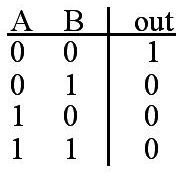
Now before analyzing the circuit using two NOR gates, we must know the truth table of the NOR gate.
From the truth table it is evident that the output of a NOR gate is zero if any of the input is 1 and the output is 1 only if both the inputs of the gate is 0.
Now to analyze the circuit let us assume that the
- SET input = 1 and RESET input = 0.
For convenience let the Set input be S and Reset input be R.
We know that if any input of NOR gate is 1 then its output is 0.
Therefore when S=1, the output of the gate corresponding to S (Gate 2 in figure) becomes 0. So Q’ becomes 0. This Q’ is given as an input (Cross coupled connection) along with R to the other gate. So the output of the second gate, Q becomes 1(since both R and Q’ are 0).
Conclusion 1: When S=1 and R=0. The outputs Q’=0 and Q=1.
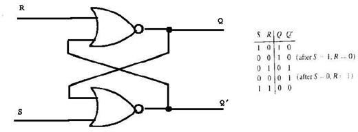
Now when the set input(S) returns to 0, the output remains the same. This is because the output of gate 1 (ie) Q is 1.Now the inputs to gate 2 are S=0 and Q=1. So from the truth table of NOR gate we can say that Q’=0.
Conclusion 2:When S=0,R=0.The outputs Q’=0 and Q=1.
- Similarly let us assume S=0 and R=1.
When R=1,Its corresponding output Q becomes zero. Since both S and Q are zero the output Q becomes 1.
Conclusion 3: When S=0,R=1. The outputs Q=0 and Q’=1.
Now when R returns to 0, the output still remains the same, because the other input to the gate(ie) Q’=1. So from the NOR truth table we can deduce that Q=0.
Conclusion 4: When S=0,R=0. The outputs Q=0 and Q’=1.
Now what happens when both Set and Reset inputs are given 1. When both S and R are given a value of 1, both the output becomes 0 which is not possible. Both the outputs cannot be 0 because we already know that the output of flip-flops are complementary to each other,one output is the complement of the other one. So we must ensure that this state is avoided and 1’s are not applied to both inputs simultaneously, during the normal operation of flip-flops.
So following points can be deduced from the above discussion.
• The outputs of the Flip-Flops Q and Q’ are complements of each other and same value cannot be obtained for both outputs.The value of normal output is nothing but the binary state of the flip-flop.
• Both the inputs of Flip-flop remains at 0 unless the state is changed by applying external pulse. When a pulse is applied to set input the flip-flop enters SET state and when a momentary pulse is applied to Reset input, the flip-flop enters CLEAR state. But we should make sure that the momentary pulse applied to set input goes back to zero before a pulse applied to reset input.When both the inputs are given a momentary pulse at same time, both the outputs become zero which is an undefined state and must be avoided.
• The Flip-flop consists of two useful states, The SET and The CLEAR state.When Q=1 and Q’=0, the flip-flop is said to be in SET state. Similarly when Q=0 and Q’=1,the flip flop is said to be in CLEAR state.
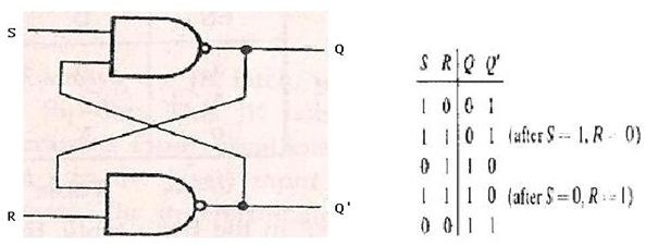
Similarly a flip-flop with two NAND gates can be formed. The truth table and logic diagram is shown below.
Thus a basic flip-flop circuit is constructed using logic gates NAND and NOR. In the next article let us discuss the various types of Flip-flops used in digital electronics.
Image and content credits:
“Digital Logic Circuits & Design” by Morris Mano