A junction refers to a place where two or more things form a connection. Find out about the PN junction and its role in semiconductor electronics
Introduction
In our previous articles we have been building the base for studying digital electronics in detail. Just to recap what we have covered till now, we started by studying the Bohr’s atomic model , quantum numbers , Pauli’s principle and energy bands. Now after covering the basic theory , we will take our first step towards learning something directly relevant to digital electronics namely a P-N junction.
The P-N Junction
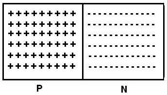
We have learnt about the semiconductor basics and know that there are two types namely intrinsic and extrinsic. The extrinsic type is further sub-divided into P-type and N-type . But have you ever thought what happens when instead of using single type we combine both these types and create a single piece which contains two halves in the form of P-type and N-type dopants. The plane which divides these two parts is obviously known as the junction since these both types meet at this plane. You can visualize a junction by taking a look at the adjacent diagram which is a very simple sketch showing such a junction. This junction is known as the P-N junction.
The Ion Guard
The above diagram is too simple and only shows an instantaneous position when the junction has just been created. After the junction is formed the actual situation changes and now instead of a plain boundary shown by the dividing line in the above sketch, we now have a more complicated state of affairs.
Let us see what is happening behind the scenes when the two junctions come in contact. We know that the p-type side has excess holes while n-type has excess electrons. And we also know that opposite charges attract each other. Hence the logical conclusion will be that the moment the both pieces form a junction, the electrons would combine with the holes and neutralize them and very soon we will have a piece which is neither n-type nor p-type but simply neutral like a normal metal. But this does not happen in the real world, so let us find out what is stopping this from happening.
This is prevented by rows of ion guard or charged ions on both sides of the junction. Actually in the beginning the electrons and holes do rush towards the opposite side and get neutralized, but very soon this gives rise to charged ions at a small region near the border or the junction. These charged ions are positively charged in the n-type region and negatively charged in the p-type region.
So now say a new electron from the n-type tries to rush to the other side, it will be absorbed by a hole on the same side which will get neutralized in turn. Suppose even if the electron somehow manages to cross the border and escape the hole, the other side has negatively charged ions which repel the similarly charged electron hence it is pushed back. This same theory applies to the holes on the other side of the border as well. This automatic flow of electrons and holes to the other sides is known as diffusion current. Hence the net result is that all the electrons and holes do not get neutralized by only a small fraction which leads to the build up of a region near the border or the junction, which consists of charged ions but is depleted from any free electrons or holes.
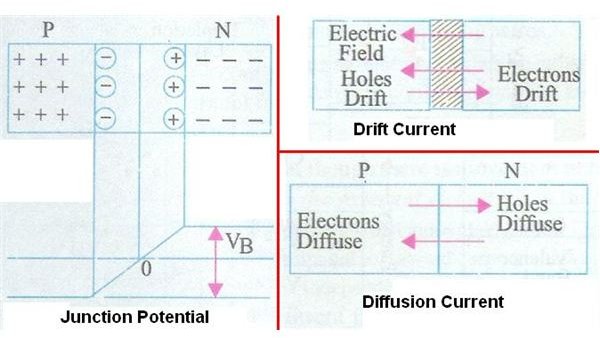
Depletion Zone
This region is known as the depletion zone or the depletion layer due to lack of charged carriers in it. Another point worth noting is that the presence of these charges also gives rise to a potential difference which prevents the further movement of free charge carriers to the other side. In this condition the drift current flows which is equal and opposite to the diffusion current and hence equilibrium is obtained. This voltage which appears automatically simply by virtue of the junction is known as junction voltage or barrier potential.
The actual value of this junction potential depends on several factors including doping density, electronic charge, temperature and so forth.