This IC is basically made up of two D-type flip flop modules and set/reset asynchronous toggle inputs. As the name suggests, the IC is primarily used as a bistable for toggling the output stage of a particular circuit, and it is fundamentally incorporated in most electronic circuits.
The IC 4013 is another important member of the CMOS IC family. They normally are available in 14-pin hermetic DIL (Dual-in-Line) ceramic package- with suffixes carrying the letters D or F. ICs in plastic packages may have the suffix “E,” and the ones which are in chip form may associate the suffix H.
IC 4013 Pin-Outs
The IC 4013 incorporates two sets of identical, discrete data-type or D-type flip flop modules. Each module is further equipped with a group of pin-outs, assigned as data, set, reset, clock inputs, and a couple of complementary outputs, Q and Q‾.
D-type flip flops refer to circuits which may have a couple of outputs that change or toggle states in response to triggers applied at the input terminals.
Pinouts of the IC
The D-type blocks consist of four inputs, explained as follows:
Complementary Ouputs (Pins 1, 2, and 13, 12): The sets of outputs change states when operated in the bistable mode or while setting and resetting the IC, always producing opposite logic levels at any instant.
Data Input (Pins 5 and 9): This input is normally connected to one of the outputs Q or Q‾ of the respective module, for the purpose of lengthening the applied signals (square wave signals) at the clock input. For other configurations this input is terminated to any of the logic levels, i.e. it’s connected either to the positive or the ground supply rail of the circuit.
Clock Input (Pins 3 and 11): This input is used for receiving clock signals which are normally in the form of square waves. The signal may be applied externally through a transistor astable multivibrator or more conventional types using NAND gates or NOR gates. The signals produces a bistable effect over one of the free outputs, the other being connected to the Data input as explained above.
Set and Reset Inputs (Pins 4, 6 and 10, 8): Following conventional safety standards, primarily these inputs also need to be assigned to a logic level, preferably to the ground terminal for the present IC, via sufficiently high value resistors. Once this is done, the inputs can be made to alternately respond to positive peak pulses to correspondingly toggle the logic states of the Q and Q‾ outputs alternately.
Positive input (Pin 14): This pin receives the positive supply input, which must never exceed 15 volts DC. Pin 7 is the ground or negative supply input of the IC.
Using the D-type as a Bistable Multivibrator or as a Flip-Flop Circuit
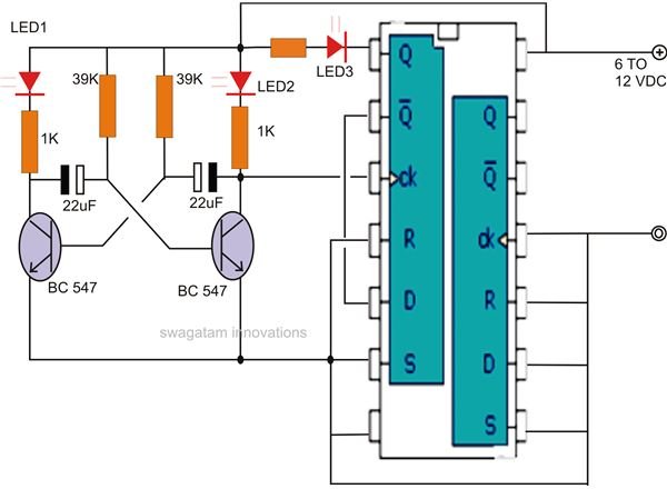
The diagram illustrates how a 4013 IC may be set up for testing its fundamental bistable operation and how it can be further applied for practical uses.
The testing is done with the following steps:
Procure the parts shown in the figure, along with the veroboard, cut into the specified size.
Gently adjust and fix the IC on the veroboard somewhere over the center of the board by soldering.
Terminate all the pin-outs as directed in the diagram by soldering the connections correctly.
After all the connections are made, have a quick glance and make sure that all have been wired as per the diagram, if possible brush-clean the solder side with thinner.
Finally connect the circuit to the specified power input. You should find the following results:
The astable starts immediately, supplying the clock pulses to the IC 4013’s clock input. The astable clocks can be witnessed through LED1.
However the output Q produces a “divide by two” output of the input clocks, presenting a perfect flip-flop action.
Here, assuming initially the clock generates a logic zero pulse, Q is off, and Q‾ being the complementary to Q, is at logic high level.
Since Q‾ is connected to the data input, it also is at a high logic level, so that now it’s ready for the toggling action.
The first positive clock input signal puts Q‾ to a logic high level, the action prompts the data input to shift its high data information to Q, switching it to a logic high (LED #2 illuminating). The action also simultaneously switches Q‾ to a logic zero, rendering the D input inactive, until the next positive clock is received when the D input is again “charged up” for the toggling action but only after the following high clock pulse (LED #2 shuts off) is detected.
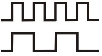
The graphical illustration of the clocks at the clock input and the Q output of the IC shows how the configuration is able to double the received clock’s time period at the Q output.
The configurations can be repeated by connecting the modules in series for getting the time period to any desired lengths, but in multiples of two.
Set Reset Actions: Yet another important feature of the IC which enables the bistable operation through two different inputs. The set up shown can be simply built with the help of the diagram.
Assuming Q‾ to be high initially, pressing S1 instantly forces the output pairs to change making Q go high. Pressing S2 now, just flips the status of the output to its original position.
Two Interesting Practical Application Circuits
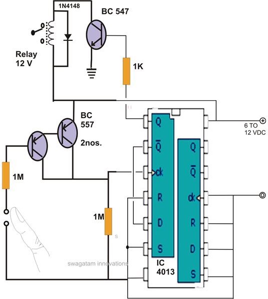
Simple Touch Operated Flip Flop Switch: The circuit shown can be used for toggling any load simply by touching the touch pad. Here we can see how the above discussed operating principle of the IC is practically set up for a useful purpose.
Clap Switch: The IC 4013 can be also effectively used for switching any load through input signals received from a sound sensor. The sound sensor here is wired up for detecting loud sound levels, like a “clap sound.” The sound hitting the mic is amplified by the transistor stage and fed to the clock input of the IC where it is processed in the same way as discussed above.

References
- Images drawn by author
- Author’s own experience
- Dual D-type Flip-Flops - http://www.doctronics.co.uk/4013.htm#pins