With monolithic linear ICs becoming commonly available, making monster power audio equipment at home has today become a child’s play. One such device STK4221 from SANYO can be simply used for different massive power audio amplifier applications. One sample circuit is discussed herein.
Circuit Description
The STK4221II IC from SANYO is a dual high power amplifier chip, preferably suited for compact high power audio applications, for example in cars and luxury transport vehicle audio systems. The chip provides a hassle free stereo output through a single package and a hand full of few external components, making the construction of this circuit rather easy and straightforward. However since the idea presented here does not include a CD or a memory card driver circuit, the input may be derived from readymade audio sources like an ipod, CD walkman, cellphone etc.
The circuit discussed here is intended specifically for car audio applications and provides a simple alternative for making a 100 watt car stereo amplifier circuit. The diagram may be understood with the following points:
An RC network formed by R5, R6 and C3, C4 together helps to reduce and filter stray frequency interferences and is therefore included at the input of the amplifiers.
Capacitors C5 and C6 are the coupling capacitors used for blocking DC. The values of these capacitors are chosen such that it does not introduce high reactance levels at low frequencies. This particularly helps to reduce the influence of the input interference noises over the signal source resistance. The value of these capacitors may also be optimized for reducing the “pop” noise when power is switched ON.
C9 and C10 determine the low cut off frequency of the circuit and may be calculated using the formula:
fɩ = 1/2π.C9.R7 (Hz)
It is recommended that C9 is suitably chosen for getting the desired voltage gain at lower frequencies. But the value should not be exceeded too much which would result in loud “pop” noises during power switch ONs.
C19 is the decoupling capacitors kept for cleaning and filtering instantaneous ripple surges during power switch ONs and providing better safety to the ICs.
C15 and C16 are the Bootstrap capacitors which introduces better response at higher frequency when smaller values are chosen and vice versa.
C17, C18 and C13, C14 are all responsible for keeping unnecessary oscillations at bay. These must be fixed as close as possible to the ICs supply rails for minimizing supply power impedance effects and to maintain stability.
Resistors R3 and R4 provide input biasing to the IC. These resistors are placed for biasing the input pins of the IC to zero potential levels.
Resistors R7, R8, R9, R10 are all used for fixing the voltage gain of the IC. Preferably R7/R8 should be selected as 560Ω and R9/R10 should be chosen as 5K6 for a voltage gain of 40dB.
The voltage gain may be adjusted by dimensioning R7 or R8 appropriately, however now the values of R3, R4, R9, and R10 will need to be made equal for maintaining proper mid-point balance.
Resistors R12 and R21 define the quiescent current level and the values recommended for the present circuit is ideally = 4K7 + 4K7.
R15 is the current limiter resistor which acts as the predriver for TR during output short circuits.
R 14 ensures correct positive/negative balance when the output shows clipping tendencies.
When the circuit is muted; TR11 is switched ON, passing current from ground to –Vcc through it. To ensure correct power dissipation during this operation, R18 and R19 must be selected as 1K/1Watt each.
L1 and L2 are included for inhibiting high-frequency oscillations at the output of the circuit.
Heatsinking for the IC STK4221
Since the IC may be run at saturating points, it is recommended to provide the device with sufficient cooling for getting optimum performance. This is done by attaching large finned type heatsinks with the IC’s fixing holes. Alternatively homemade heatsink in the form of 6 × 5 × 0.4 inches aluminum plates drilled appropriately may also be used for sustaining optimum performance.
Though as per calculations the heatsink required was quite bigger than the above specs, practically it is chosen as above because the input music signal varies a lot and the IC is fully loaded only during intermediate peak levels and not throughout the operation.
The thermal resistance of the heatsink (Ɵc-a), for STK4221’s power dissipation (Pd) may be determined with the below given couple of conditions:
-
Tc = Pd × Ɵc-a + Ta ≤ 1250 C
-
Tj = Pd × Ɵc-a + Pd/4 × (Ɵj-c) + Ta ≤ 1500 C
Where Ta = Recommended ambient temperature,
Tc = Working case temperature and Tj = Device’s junction temperature.
Power Supply
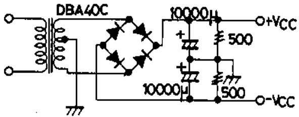
A typical dual power supply configuration shown below can be employed for powering the proposed 100 watt stereo car amplifier circuit. The diagram shows a center tap transformer suitably wired up with a standard bridge network and a couple of high value electrolytic filter capacitors for the required dual supply outputs.
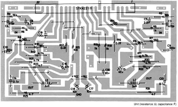
The whole circuit can be easily built without facing any trouble whatsoever, if it’s assembled over the specified PCB design shown below. The completed circuit can be accommodated inside an appropriately ventilated metal enclosure along with the power supply if intended for external use or inside a plastic sleek looking housing for vehicular installations with power being taken from the vehicle battery itself.
Reference
SANYO Datasheet - STK4221