Sputter Deposition is a thin film deposition and surface coating technique that exploits the sputter phenomenon to achieve thin film development. An enhanced variation of the technique, Magnetron Sputter Deposition, uses magnetic fields to achieve higher yields and better performance.
Introduction
One of the main methods used for depositing thin films onto substrates is Sputter Deposition. The technique is used for the coating of a variety of materials such as metals, semiconductors and insulators, both in an industrial and a lab-scale level. A variation of this technique, the Magnetron-Sputter Deposition, can provide better sputtering rates and higher yield by effectively utilizing and combining strong electric and magnetic fields during the sputter process.
Sputtering: What is it?
When a solid material surface is being bombarded with energetic particles (e.g. accelerated ions), a cascade of collisions takes place, causing a number of surface atoms to eject from the target material and follow random trajectories. This simple phenomenon is called sputtering.
Aside from the ejected atoms, the emission of secondary electrons from the target material also takes place. These secondary electrons are necessary in order to sustain the plasma (glow discharge phenomenon) and maintain the deposition process as explained below.
The Sputter Deposition Process in General
Many of the techniques developed for depositing thin films take advantage of the sputter phenomenon. The main system used by these techniques consists of a pair of planar electrodes, the anode where the substrate (e.g. silicon wafer) is placed, and the cathode (target) that is made up of the material that will be used for the thin film deposition onto the substrate. The two electrodes are located inside the low pressure vacuum deposition chamber (~0,1 Torr). This is a chamber filled with the sputtering gas, usually an inert gas such as Argon (Ar).
Once negative voltage is applied to the target surface, any existing Ar positive ions will accelerate towards the cathode and after falling on it, a small stream of atoms or clusters of atoms will eject from the cathode material. A small portion of them will impact on the anode’s wafer, leading to the formation of a thin film onto the substrate. In order to keep the process going, constant gas ionizations are necessary and this is achieved with the aid of the secondary electrons that collide with neutral atoms and generate new ions.
The sputter yield S is provided by the following equation:
S = (atoms removed)/ (incident ions)
and is highly dependent on the:
- incident ion’s energy,
- target material,
- incidence angle and
- target structure.
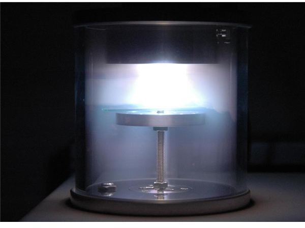
Sputter Chamber With a Visible Plasma Discharge
Why Magnetron Sputtering?
In order to increase performance, variations on the basic principle have been developed. One of the many variations involves the use of a magnetic field close to the cathode’s plane. The secondary electrons generated during the sputter process are trapped by this field and stay close to the cathode surface. Following helical paths around the magnetic field lines, these electrons are forced to travel longer distances inside the chamber and thus induce more ionizations and finally increase the sputter yield S in a significant degree.
The use of this variation has certain advantages. It allows for an increased sputter rate, higher plasma density, and the ability to sustain plasma at lower pressure, meaning that less gas is needed in the vacuum chamber.
Summing Up
By modifying various parameters, it is possible to deposit almost all kinds of materials. The use of DC power supply as described above is suitable for metal targets, while the use of RF or pulsed DC supply enables the use of semiconductors and insulators as targets as well. Also, the use of a reactive instead of an inert gas (reactive sputtering), enables the chemical reaction between the gas and the target material and thus the deposition of a compound thin film onto the substrate.
These controllable variables, make the Magnetron-Sputter technique very efficient compared to other deposition methods and suitable for almost every target material.
Sources:
- PVD-Coatings: How Are PVD Coatings Deposited
- Sputter Deposition For Thin Films
- “Surface-Thin Film Science”, LTFN, 2006