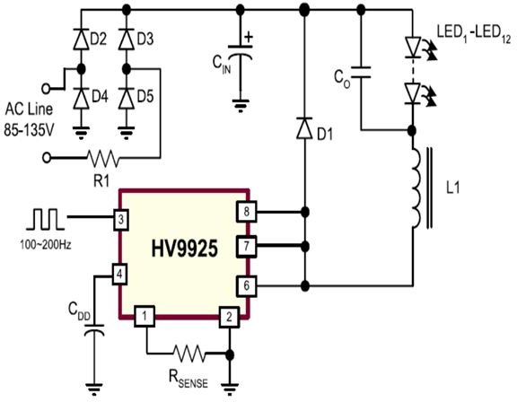
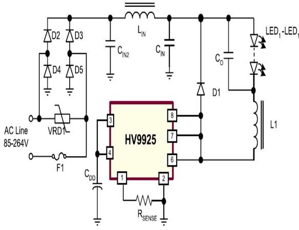
How to Build a PWM Programmed Power Saving White LED Driver Circuit
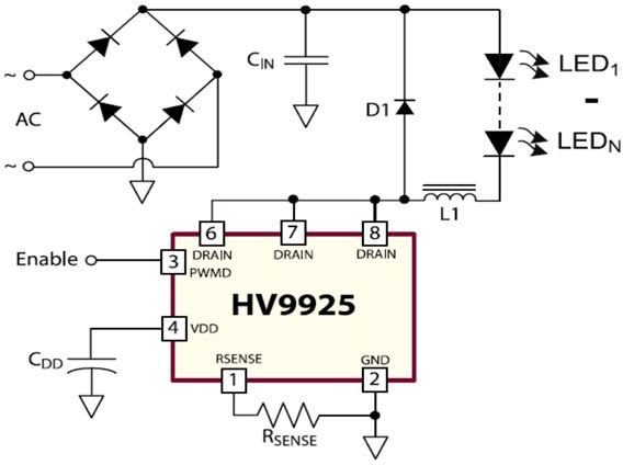
The IC HV9925 from Supertex Inc. is a high-efficiency LED driver/controller device equipped with a unique PWM switched LED dimming facility. The PWM programming helps to save LED power making the circuit extremely power efficient and long lasting. The device is especially designed for driving the vulnerable high-bright white LEDs from input voltages ranging as high as 400 VDC.
The IC provides a current controlled output supply to the connected LEDs (upto 12 nos.) which ensures uniform illumination and high endurance of the LEDs.
The IC requires a very few external components for performing the required operations.
In the proposed circuit, IC HV9925 acts as a PWM peak current controller which also drives a buck boost configuration through continuous conduction mode (CCM). The design of HV9925 assures control of the converter’s output current instead of the voltage, which is programmable through a single resistor fixed externally (R_sense_). The design works more efficiently with groups of LEDs connected at the output and thus suits applications where high illuminations at low consumptions are required.
One of the pin-outs inputs designated PWMD enables dimming of the LEDs through PWM - one of the key features of the circuit.
When the voltage across R_sense_ tends to rise above 0.47V, a switch cuts off and pulls the “DRAIN” output to a high impedance level, also simultaneously activating a single shot circuit which sets the delay-off period of the switch to about 10.5µs.
Application Clues and Parameters
The following information provides important tips for selecting and calculating the various components assumed to be critical with the present application:
Calculating L1 and D1
The inductance of L1 required for the application is inversely proportional to the present ripple current ∆I₀. For checking noise interference in the current sense comparator it becomes favorable to set the peak-to-peak ripple at 20 to 30%.
Therefore L1 = (V₀.Toff) / ∆I₀
where V₀ = forward voltage drop of the entire LED series, Toff = is the internally set off-time of the chip.
In the above expression the unknown I₀ is calculated as
I₀ = (VTH/Rsense) – 1/2∆I₀
where VTH is the internal set threshold of the current sense comparator. An peak-to-voltage malfunction presented at the output current set-up requires attention. The constant off-time feature employed in the IC keeps the ripple current almost independent of the input voltage changes, which in turn keeps the output voltage unaffected from these input variations.
In case further ripple current elimination is felt necessary, this may be done simply by adding a capacitor across the connected LED string, which also means that now L1 can be selected with relatively lower values. However, since the peak-to-average current gets influenced by Toff variations, the initial current output might not be accurate at bigger ripple currents through L1.
Other factors connected with the present LED driver design are the various associated external parasitic influences caused through L1’s distributed winding capacitance, junction capacitance, capacitances generated from PCB board traces and from output capacitance C(drain) of the circuit itself.
The total parasitic capacitance can be expressed as:
Cp = C(drain) + C(pcb) + Cɩ + Cj
In the view of eliminating the above parasitic effects, the manufacturer has recommended certain guidelines which must be followed while making this LED light driver circuit. Let’s learn them with the following instructions:
L1’s coil capacitance needs to be optimized by referring to the manufacturer’s data book or according to the standard self-resonant formula, given as:
SRF = 1/{2π√(L.Cɩ)}
Where L is the inductor’s value, Cɩ is the coil capacitance.
The capacitance Cɩ might generate a fair bit of spikes during constant switching actions, which might not be safe for the connected LED string. The spikes however can be canceled out by attaching a capacitor across the LED series, the value being somewhere close to 10 nF.
The manufacturer of the IC HV9925 recommends the incorporation of super-fast rectifier diodes for D1 to increase efficiency and eliminate chances of spurious triggering of the current sense comparator stage.
Diodes specified with quick reverse recovery time and minimum junction capacitance Cj, exhibits improved performances.
The diode must be rated with greater reverse voltage Vʀ handling capacity than the applied maximum input voltage across the LEDs.
During switch ONs, Cp discharges a current of 150ma (typical) into the drain output of the IC. However with an increase in the junction temperature, the current may show reducing tendencies.
The rising edge duration of the current spike can be approximately calculated as:
T(spike) = {(Vin.Cp)/I(sat)} + trr
The false triggering tendencies of the current sense comparator can be reduce by controlling Cp to the minimum as per the formula:
Cp < Isat × {Tblank(min) – trr} / Vin(max)
Where Tblank(min) = 200ns is the minimum blanking time, and Vin(max) is the maximum instantaneous voltage.
Power Loss Through Switching
The discharging of Cp into the DRAIN output of the IC introduces a significant level of power loss in the circuit as a result of the switching. This power loss can be expressed with the formula:
P(sw) = [ Cp Vin²/2 + Vin I(sat).trr].Fs
Where Fs denotes the switching frequency and I(sat) represents the saturated DRAIN Current of the HV9925 IC output.
The switching frequency Fs can be given as (ignoring voltage drops across Di and the IC)
Fs = Vin –V₀ / Vin.T(off)
When the selected input is AC, applied to a bridge rectifier, the power loss through switching may be calculated as:
P(switch) ≈ ½.T(off) (V(ac).Cp + 2I(sat).trr)(Vac - V₀), where V(ac) is the input AC line voltage.
When powered using a DC source, conduction power loss can be expressed as:
P(cond) = {D.I₀².R(on)} + Idd.Vin.(1-D)
Where D represents the duty ratio and is = V₀/Vin, R(on) is the ON resistance, Idd is the internal current for linear regulation.
More innovative ideas to save LED power using the ICs PWM programming feature is explained in the datasheet of the device, where the entire circuit parts calculations are also thoroughly discussed through practical examples.
References
- Programmable-Current LED Lamp Driver IC with PWM Dimming from Supertex Inc. - http://www.supertex.com/pdf/datasheets/HV9925.pdf