Types of flip-flop circuits explained - RS, JK, D & T
Introduction
So far we have discussed about the basics, triggering and the basic circuit of flip-flops. Now let us see the types of flip flop circuits that are being used in digital circuits. They can be classified according to the number of inputs they possess and the manner in which they affect the binary state of the flip-flop.
Types of Flip-Flops
• RS flip-flop
• JK flip-flop
• D flip-flop
• T flip-flop
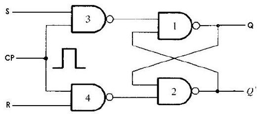
RS flip-flop
This type of flip-flop is very similar to the one we discussed in the basic circuit. But however a certain difference exists. In this flip-flop circuit an additional control input is applied. This additional control input determines the when the state of the circuit is to be changed. This additional input is nothing but the clock pulse.
The RS flip-flop consists of basic flip-flop circuit along with two additional NAND gates and a clock pulse generator. The clock pulse acts as an enable signal for the two inputs. The output of the gates 3 and 4 remains at logic “1” until the clock pulse input is at 0.This is nothing but the quiescent condition of the flip-flop. Now let us see how it works.
Information from S and R is allowed to reach the output only when clock pulse goes to 1.
Let’s assume S=1, R=0 and CP=1. The set state is reached at this condition and since the clock pulse is 1, information from S and R is allowed to reach output.
From the truth table of NAND gate we can say that the output is 0 only when both the inputs are 1. In all the other case the output is 1.
So when S=1, R=0 &CP=1. Both the inputs to the gate 3 are 1 and hence its output is 0. This information (i.e.) 0 is passed to gate 1. Since one of the inputs of gate 1 is 0, we can say that the output Q=1. Since R=0, the output obtained at Q’=0.
Conclusion: When S=1, R=0 & CP=1 => Q=1 and Q’=0.
Now to change to reset state, the inputs must be S=0, R=1 & CP=1. The observed outputs are Q=0 & Q’=1.When the clock pulse returns to zero, the circuit remains in its previous state. This is applicable to both Set and Clear states.
Now when CP=1, inputs S=0 &R=0, that is when both the inputs are 0, the state of the circuit does not change.
When CP=1, S=1 & R=1, an indeterminate condition occurs. Because both the outputs Q and Q’ remain at 1. This is not possible because both the outputs are complementary to each other. So it is better to avoid this condition during practise.
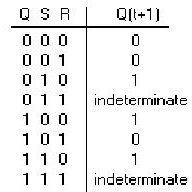
These results can be compared with those in characteristic table; Where S and R are inputs. Q is the output and Q (t+1) shows the next state. The characteristic table should be interpreted as: for the given present state Q, the inputs S and R, the application of a single clock pulse CP causes the flip-flop to go to the next state. So CP is not indicated in the characteristic table.

The characteristic equation shows the value of the next state as a function of inputs and the present state. In the characteristic equation, the indeterminate states are marked as don’t cares in the map.
D Flip-Flop
D flip-flops are used to eliminate the indeterminate state that occurs in RS Flip-flop. D flip-flop ensures that R and S are never equal to one at the same time. The D flip-flop has two inputs including the Clock pulse. D and CP are the two inputs of the D flip-flop.
The D input of the flip-flop is directly given to S. And the complement of this value is given as the R input. Similar to Rs flip-flop, the outputs of gate 3 and 4 remain at logic “1” until the clock pulse applied is 0. The value of D won’t affect the circuit until Cp is in 0. The value of D is sampled only when CP goes from 0 to 1. Now as soon as the value of Cp changes to 1, the value of D is sampled and the information is passed to the output.
Now assume that CP=1. Now if D=1, the output of gate 3 goes to 0 and this makes the output Q=1, Q’=0. This is the set state of the D flip-flop. When D=0, the output Q’=1 and Q=0, which is the reset state of the Flip-flop.
Since both S and R are given complementary values they can never be 1 at the same time. Thus we can avoid the indeterminate state that occurs in RS flip-flop.
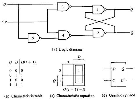
When the clock pulse returns to zero, the previous state of the output is maintained (or) the output does not change its state unless it is enabled again by clock pulse. This Flip-flop is sometimes called Gated D-latch.
From the characteristic table it is evident that the value of Q (t+1) is independent of the value of Q and also the value of D and Q (t+1) are one and the same. So it is quite clear that the clock pulse transfers the value of the input directly to the output regardless of the value of output before the Clock pulse was applied.
In the next article let us discuss the other two types of flip-flops.
Image and Content Credits:
“Digital Logic Design” by Morris Mano.