How to Build a 100 Watt MOSFET Amplifier Circuit - Simple Design Explored
MOSFET vs. Normal Transistors
MOSFET is the acronym for Metal Oxide Semiconductor Field Effect Transistor. Just like any other transistor MOSFETs are also bipolar semiconductors, but have a significant edge and are the more advanced or enhanced version of normal transistors.
The positive temperature coefficient found in MOSFETs is a very interesting characteristic they have. This feature makes it sure that the current through them decreases with an increase in their case temperature.
Therefore, when these transistors are connected in parallel, any disproportionate rise of temperature among them is effectively distributed and compensated by an overall decrease in the current flow through them and the heat in turn is regulated. Normal transistors would easily be destroyed under such circumstances due to a thermal runaway situation.
MOSFETs are also specifically designed for handling high currents to produce large power outputs and therefore are extensively used in inverters and compact high power amplifier module circuits.
One such MOSFET amplifier circuit is presented here, which is very compact in design, yet is able to produce a power output of as high as 100 watts.
Let’s find out how the circuit functions.
Circuit Description
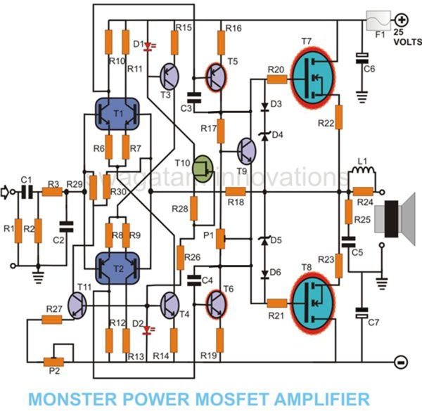
Referring to the circuit diagram (click to enlarge), we see that the design of the amplifier is symmetrical and all transistors operate in a class A configuration.
-
T1 and T2, included in the differential input stages are dual pack transistors and thus are perfectly matched.
-
Transistors T4 and T3 are arranged as current sources for proper regulation of T1 and T2 respectively.
-
LEDs D1 and D2 are used to produce reference voltages for T3 and T4. LEDs are specifically preferred in place of zener diodes because of their low noise characteristics.
-
T3/D1 and T4/D2 should be coupled (physically attached) to each other to promote thermal stability. Clamping is advised, but not an absolute criterion.
-
Due to the slight difference in the current amplification of T1 and T2, bias correction at the input stage becomes essential. T11 is introduced just for the above purpose.
-
T11 gets the required reference voltage source from D2 and the output voltage is set to 0 volts with the help of preset P2.
-
The inclusion of coupling capacitor C1 at the input correction stage becomes necessary, but practically it poses no problem as the measured cut OFF frequency is found to be not more than 1.5 Hz.
-
A low-pass filter comprising of R3 and C2 are appropriately dimensioned to cancel out frequencies above 300 KHz. This takes care of TIM (Transient Inter-Modulation) distortions and many other stray RF disturbances.
-
The signals from the input stage is sufficiently amplified by transistors T5 and T6 in the Cascode stages.
-
The amplified signal is used to drive the output MOSFETs comprising of T7 and T8 which are connected as push-pull high power, high gain amplifier.
-
Transistor T9 is kept to compensate for any abnormal increase in the gate current of the MOSFETs.
Construction Tips
Although a PCB layout is not available, with little care and concentration the present single MOSFET amplifier circuit may be built over a general purpose PCB as was done by me a couple of years ago.
The construction procedure may be completed by following the below given points:
-
Since a general PCB is being used, begin by inserting all the general purpose transistors consisting of T1, T2, T3, T4, T9, T10 and T11 over the PCB, by approximating the distances between them as per the circuit diagram.
-
Solder their leads to fix them over the board. Similarly, distribute by inserting all the other associated passive components around the transistors, interlink them by soldering with the help of the circuit schematic.
-
Finally, fix through soldering the power transistors and the MOSFETs, such that they are situated at the edge of the PCB, with their metallic side facing outwards. This is required to facilitate the fitting of a common heat sink to these transistors. Do not forget to use mica isolation kit and heat sink compound while fixing the heat sinks.
-
Interconnect each and every connection and recheck to confirm correct wiring.
Parts List
All resistors are ¼ watt CFR unless otherwise specified.
R1 = 1M,
R2,27 = 47K,
R3, 20, 21 = 470Ω,
R10, 11, 12, 13, 28, 17 = 1K,
R6, 7, 8, 9 = 56Ω,
R29,30 = 330K,
R14,15 = 270Ω,
R26 = 4K7,
R16,19 = 100Ω,
R18 = 22K
R22,23 = 0.25/2W, WIRE WOUND
R24 = 1Ω,
R25 = 10Ω,
P2 = 47K,
C1 = 2µ2,
C2 = 1 nF,
C3,4 = 10 Pf,
C5 = 47 nF,
C6, C7 = 100µ/50V,
C8,9 = 10,000/63v,
D1,2 = LED RED,
D3,6 = 1N4148,
D4,5 = 12V/400mW,
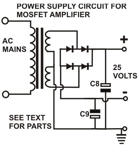
Power Supply Diodes = 6 Amp. 300V
T1 = MAT 02,
T2 = MAT 03,
T3 = BC 560C,
T4 = BC550C,
T5 = BF 470,
T6 = BF469,
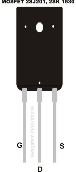
T7 = 2SK 135,
T8 = 2SJ 50,
T10 = BF256
T11 = BC550
L1 = 20 TURNS OF 0.8mm COPPER WIRE OVER R24,
FUSE = 10 AMPS. SLOW BLOW,
GENERAL PCB,
MICA ISOLATION KIT FOR THE RELEVANT TRANSISTORS
HEATSINK FOR T5,6,7,8 = < 1K/W
TRANSFORMER = 25 – 0 – 25 / 5A.
Setting Up the Unit
Once you have completed the construction of the circuit board, the setting up of the amplifier may be easily done through the following steps:
-
Before connecting the power supply to the unit, make sure that P1 is fully turned clockwise.
-
Do not connect anything (speaker) at the output as yet and also keep the input terminals shorted externally.
-
Without inserting the fuse into the socket, connect the power supply to the circuit and switch it ON.
-
Take a digital multimeter, set it to the 1A DC range and connect its prods to the fuse terminals with the red prod going to the positive end.
-
If all the connections are made correctly, the meter should read a current of not more than 100 mA. If its more than that, definitely something’s wrongly connected, so recheck to identify the fault.
-
After the fault is rectified, adjust P1 so that the meter reads just about 50 mA. This fixes the quiescent current of the circuit.
-
Insert the specified fuse into its socket.
-
Next, set the DMM to a double digit DC volts range, measure the voltage across resistor R22 and adjust P1 to make it read near about zero volts.
-
The above operations should set the unit up perfectly.
-
Now you may go on to connect a loudspeaker at the output terminals and feed an input music. A highly amplified music should be instantly audible over the loudspeaker. Optimize the source volume as per taste.
The raw power of this single MOSFET amplifier circuit, along with some chillingly crystal clear output is sure to give you an “out of this world” experience.